目录
ToggleIntroduction to Intel's PCB Tabbed Routing Technology and Solutions
Introduction
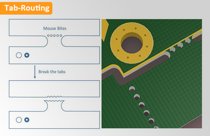
PCB Tabbed Routing, developed by Intel, is an innovative technique designed to optimize signal integrity and reduce crosstalk in PCB designs, especially in space-constrained environments. By incorporating small tabs into the transmission line structure, this method effectively addresses impedance mismatches and signal interference issues. Primarily applied to DDR bus layouts, Tabbed Routing offers a unique solution to common PCB design challenges.
Why Use Tabbed Routing?
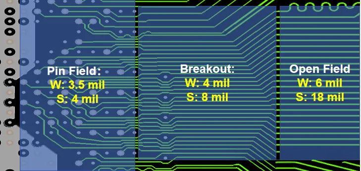
To understand the need for Tabbed Routing, it’s essential to grasp the characteristics of DDR bus routing and key concepts like Pin Field, Breakout, and Open Field. These terms describe different PCB routing areas, crucial for implementing Tabbed Routing.
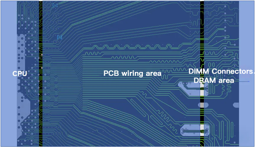
DDR PCB layouts typically consist of three main sections: the CPU area, the routing area, and the DIMM connector or DRAM area. Within these sections, the Pin Field represents the BGA pad and via region, where limited space necessitates narrower trace widths and reduced spacing, leading to increased impedance and crosstalk. Similarly, the Breakout area requires compact routing to fan out DDR signals, also resulting in higher impedance and crosstalk.
Principle and Simulation of Tabbed Routing
Tabbed Routing addresses two primary issues:
- Reducing impedance to improve impedance matching and minimize signal reflection.
- Reducing far-end crosstalk (FEXT) by altering the capacitive characteristics of transmission lines.
Adding tabs effectively increases the trace width, thereby lowering the impedance and aligning it more closely with the desired value. Additionally, adjusting the capacitive properties through tabs helps reduce crosstalk between signal lines.
A practical example from Intel’s documentation demonstrates the impact of Tabbed Routing on far-end crosstalk. For a pair of microstrip lines with an 8-inch coupling length, the introduction of tabs reduced the crosstalk amplitude from 42 mV to 2 mV, showcasing significant improvement.
Table: Impact of Tabbed Routing on Far-End Crosstalk
| Configuration | Far-End Crosstalk (mV) |
|---|---|
| Without Tabbed Routing | 42 |
| With Tabbed Routing | 2 |
Practical Design and Application
Tabbed Routing can be applied in two main areas: the Pin Field and the Breakout region (also known as Interdigital Tabbed Routing). By strategically adding tabs in these areas, designers can achieve impedance compensation and reduce far-end crosstalk, leading to better signal integrity.
Modern PCB design tools like Allegro include plugins for automated Tabbed Routing design, allowing designers to input specific parameters and generate optimized layouts efficiently.
Conclusion
Tabbed Routing, pioneered by Intel, offers a powerful solution for overcoming space constraints in PCB design. By improving impedance matching and reducing crosstalk, this technique enhances the overall signal performance of DDR PCBs. Its application extends beyond PCB design to include packaging and interposer designs, making it a versatile tool for modern electronic engineering.