Mastering PCB Pad and Solder Mask Design Essentials
Key considerations for effective PCB pad and mask design.
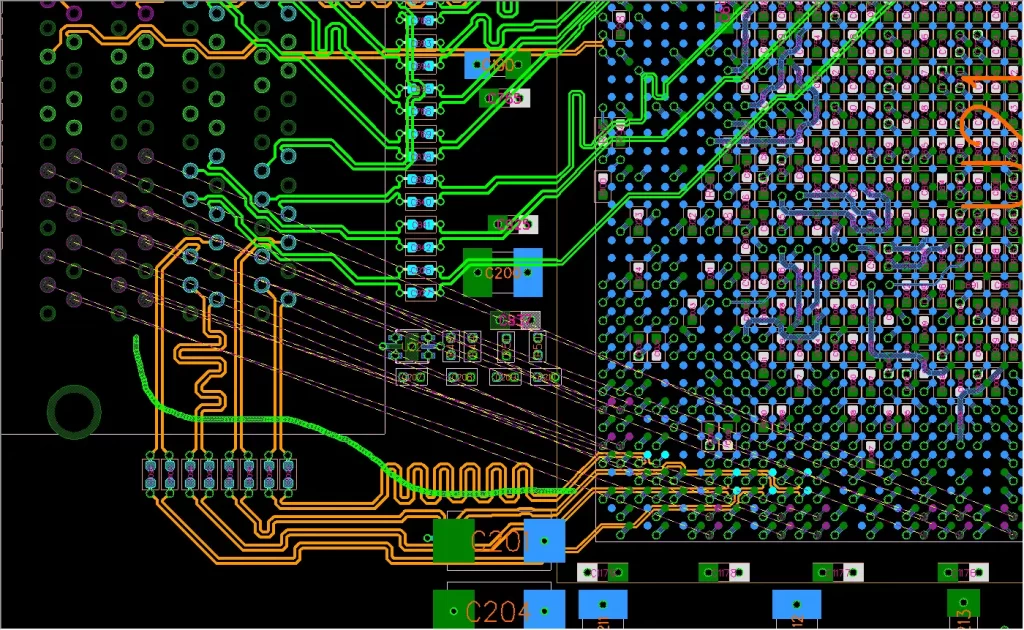
Essentials of PCB Pad Design:
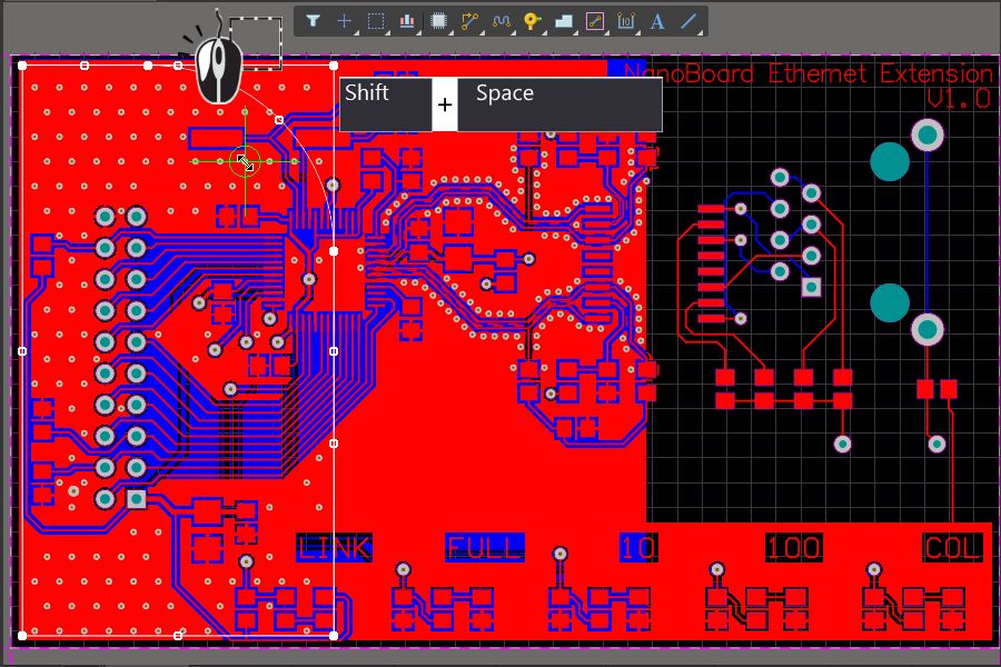
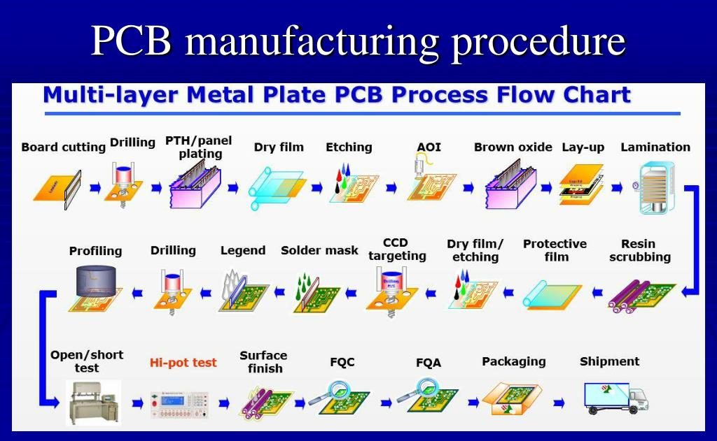
In PCB manufacturing, pad design encompasses various considerations such as plated and non-plated through-hole pads, each influencing the manufacturing capabilities of the PCB.
During PCB fabrication, factors like film and material expansion, compression during lamination, and precision in drilling hole positions can lead to misalignment between layers. To ensure proper interconnection between layers, the width of solder mask pads must consider interlayer alignment tolerances, effective insulation clearances, and reliability requirements, reflecting in controlled pad widths.
- Width Guidelines for Different Pad Types:
- For plated through-hole pads, a width of 5 mil or greater is recommended.
- Thermal relief widths typically range around 10 mil.
- Outer layer solder mask pad widths for plated through-holes should exceed or equal 6 mil to accommodate solder mask requirements.
- Inner layer solder mask pad widths for plated through-holes should exceed or equal 8 mil to meet insulation gap requirements.
- Non-plated through-hole solder mask pad widths are generally designed around 12 mil.
Insights into Solder Mask Design:
Determining factors such as minimum solder mask clearance, minimum solder mask bridge width, and minimum solder mask expansion depend on solder mask transfer methods, surface treatment processes, and copper thickness. For more precise solder mask designs, consultation with PCB manufacturers is recommended.
- Recommended Dimensions for Solder Mask:
- Under conditions of 1oz copper thickness, a solder mask clearance greater than or equal to 0.08mm (3 mil) is advised.
- Under conditions of 1oz copper thickness, a solder mask bridge width greater than or equal to 0.10mm (4 mil) is suggested. When employing immersion tin surface treatment, the solder mask bridge width should be moderately increased, typically to a minimum of 0.125mm (5 mil), due to the attacking effect of the immersion tin solution on certain solder masks.
- Under conditions of 1oz copper thickness, a minimum expansion size of 0.08mm (3 mil) for conductor Tm covers is recommended.
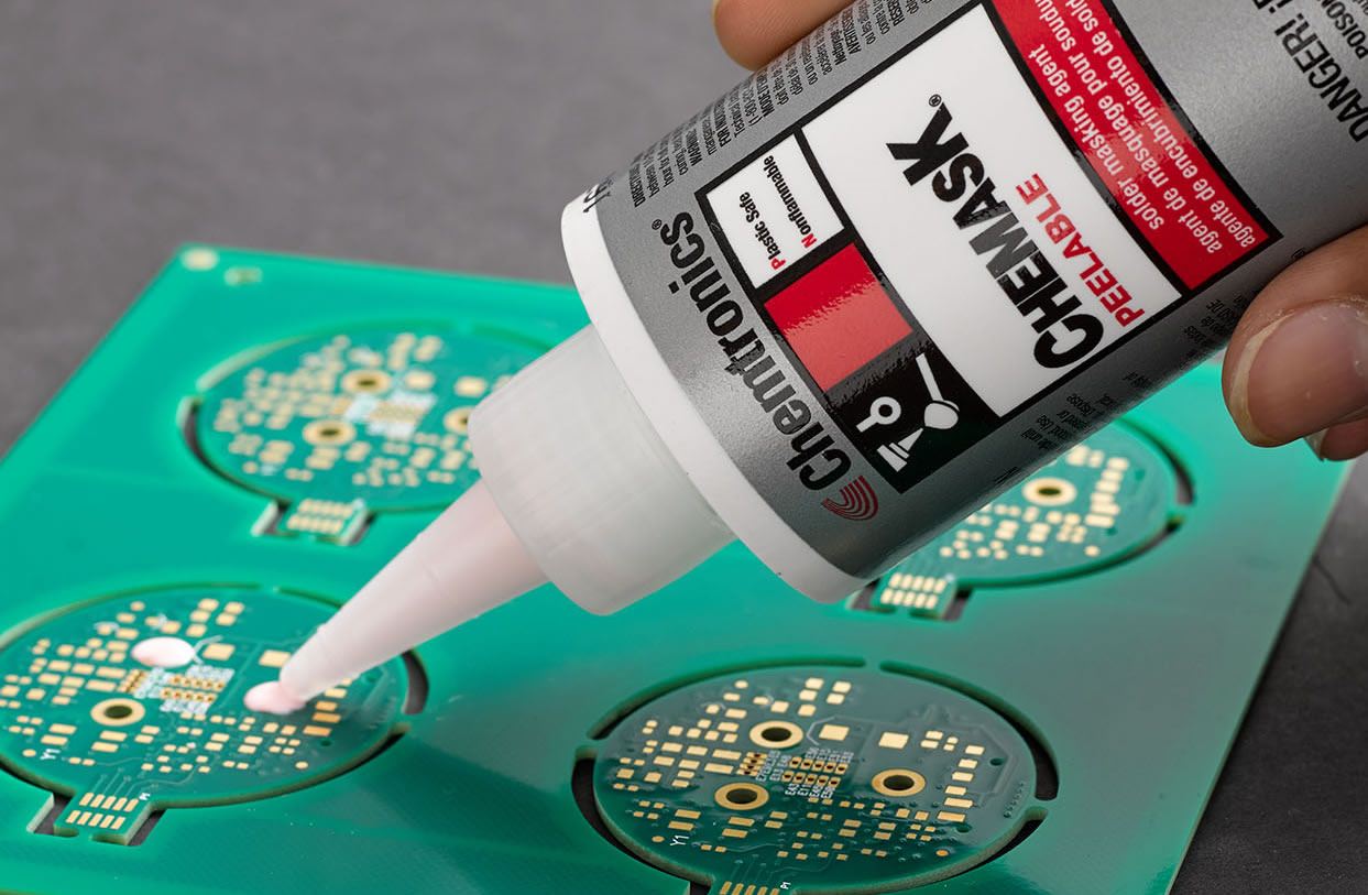
Solder mask design for vias is a critical aspect of PCBA manufacturing feasibility design and depends on the process path and via layout.
- Common Solder Mask Methods for Vias:
- Plugging (including partial and full plugging), small window opening, and full window opening are the main methods.
- For vias under BGA pads, plugging is preferred to minimize solder mask misalignment during BGA reflow soldering and reduce the risk of solder protrusion and reflow affecting reliability.
In summary, mastering PCB pad and solder mask design essentials is crucial for ensuring manufacturability and reliability in PCB manufacturing processes.