目录
ToggleIntroduction: Exploring the PCB Assembly Process
Printed Circuit Board (PCB) assembly is a crucial step in the manufacturing of electronic devices. It involves the process of mounting electronic components onto a PCB, creating a functional and reliable circuit. Understanding the PCB assembly process is essential for designers, engineers, and manufacturers to ensure the successful production of high-quality electronic devices.
Designing the Perfect PCB: Key Considerations and Best Practices
Designing a PCB is a critical step in the assembly process, as it lays the foundation for the functionality and performance of the final product. Several key considerations and best practices should be followed to ensure the design of a perfect PCB.
Firstly, it is important to consider the size and shape of the PCB. The dimensions of the PCB should be optimized to fit within the constraints of the final product while allowing for efficient assembly and testing. Additionally, the shape of the PCB should be designed to minimize signal interference and maximize the use of available space.
Another crucial consideration is the selection of components. Choosing the right components for the PCB is essential for its functionality and reliability. Factors such as component compatibility, availability, and cost should be taken into account. It is also important to consider the thermal characteristics of the components to ensure proper heat dissipation.
Furthermore, proper placement of components on the PCB is vital. Components should be arranged in a logical and organized manner to minimize signal interference and facilitate efficient assembly. Careful consideration should be given to the placement of high-frequency components and sensitive analog components to avoid noise and signal degradation.
Lastly, adherence to design for manufacturability (DFM) guidelines is crucial. DFM guidelines ensure that the PCB design is optimized for efficient and cost-effective manufacturing. By following DFM guidelines, designers can minimize the risk of manufacturing defects and reduce production costs.
From Prototype to Production: Navigating the PCB Manufacturing Process
Once the PCB design is finalized, the manufacturing process begins. This involves several steps, including fabrication, component procurement, assembly, and testing.
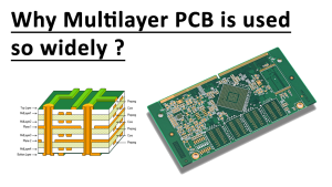
The fabrication process starts with the production of the bare PCB. This involves etching a copper-clad laminate to create the desired circuit pattern. Advanced fabrication techniques, such as multilayer PCBs and surface mount technology (SMT), have revolutionized the manufacturing process, allowing for smaller and more complex PCB designs.
Component procurement is another crucial step in the manufacturing process. Components need to be sourced from reliable suppliers to ensure their quality and availability. It is important to establish strong relationships with suppliers to ensure timely delivery and avoid production delays.
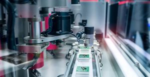
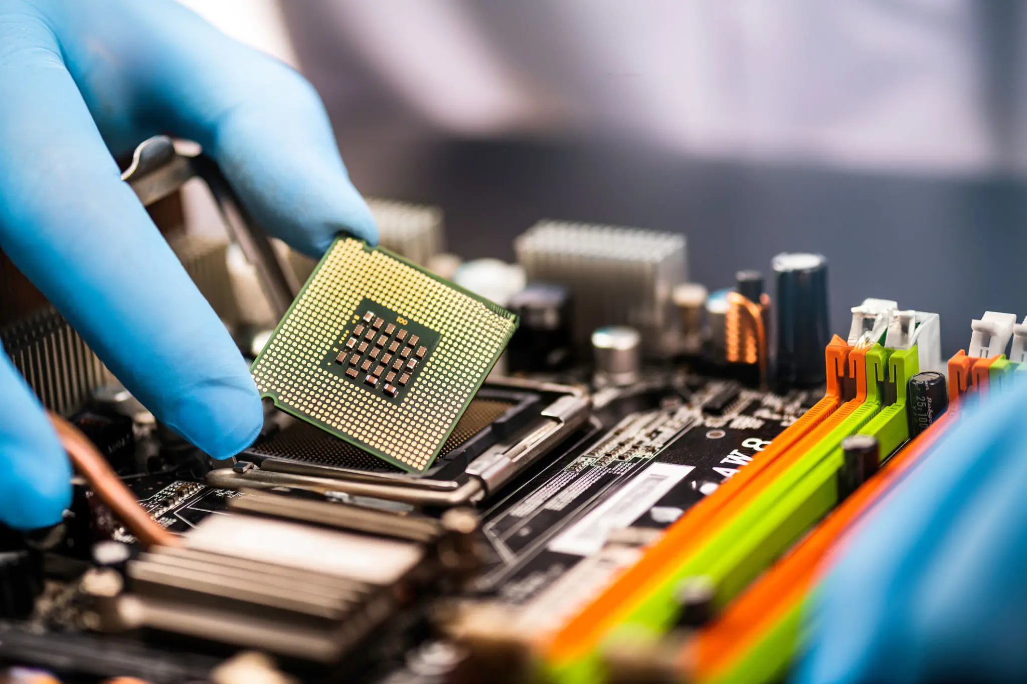
The assembly process involves mounting the components onto the PCB. This can be done through manual or automated assembly techniques. Automated assembly, such as pick-and-place machines, offers higher efficiency and accuracy, especially for complex PCB designs. However, manual assembly may be preferred for low-volume production or specialized components.
Quality Control and Testing: Ensuring a Successful PCB Assembly
Quality control and testing are essential steps in the PCB assembly process to ensure the functionality and reliability of the final product. Several quality control measures and testing techniques are employed to identify and rectify any manufacturing defects.
Visual inspection is the first line of defense in quality control. Trained technicians visually inspect the PCBs for any visible defects, such as soldering issues, component misalignment, or physical damage. Automated optical inspection (AOI) systems are also used to detect defects that may not be visible to the naked eye.
Functional testing is another crucial step in the quality control process. This involves subjecting the assembled PCBs to various tests to ensure their functionality. Tests may include power-on testing, functional testing of individual components, and environmental testing to assess the PCB’s performance under different conditions.
In addition to functional testing, reliability testing is performed to ensure the long-term durability of the PCB. This may include accelerated life testing, thermal cycling, and vibration testing to simulate real-world operating conditions and identify any potential weaknesses in the design or assembly.
In conclusion, understanding the PCB assembly process is essential for the successful production of electronic devices. Designing the perfect PCB involves considering factors such as size, component selection, placement, and adherence to DFM guidelines. Navigating the manufacturing process involves fabrication, component procurement, assembly, and testing. Quality control and testing measures ensure the functionality and reliability of the final product. By following best practices and employing rigorous quality control measures, manufacturers can achieve high-quality PCB assemblies that meet the demands of the ever-evolving electronics industry.
https://www.tf-pcb.com/services/pcb-assembly/
https://www.facebook.com/profile.php?id=100086889766737