目录
ToggleMastering the Craft of Inverter PCB Development
Navigating the Complexities of Inverter Circuit Design
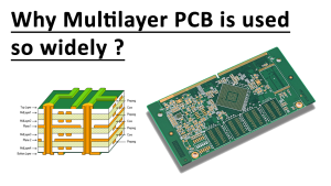
1. Basic Design Principles
This section introduces the fundamental principles of inverter PCB design, including the choice of components and the layout for basic inverter circuits. Emphasis is placed on the importance of understanding electronic principles to achieve efficient and reliable designs.
2. Advanced Design Techniques
Moving beyond basics, this part explores advanced design techniques. Topics include the integration of sophisticated components such as MOSFETs and microcontrollers, and how these elements contribute to the overall efficiency and functionality of the inverter.
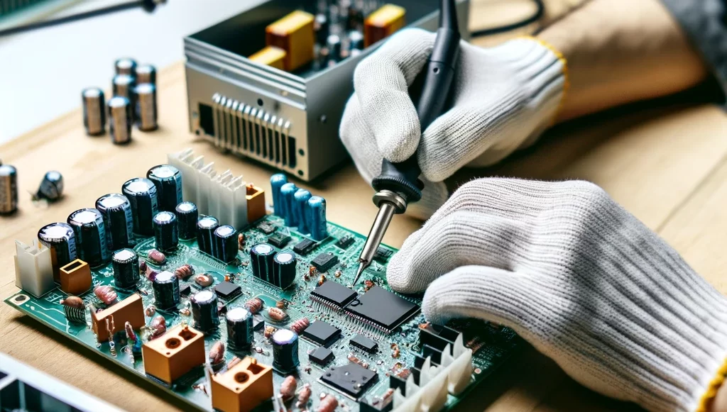
3. Assembly and Soldering
Here, the focus shifts to the assembly process, specifically the soldering of components onto the PCB. The article covers techniques for ensuring a high-quality assembly, including soldering tips and the importance of a clean working environment.
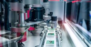
4. Quality Testing
Quality testing is a crucial step in PCB development. This section details the various testing methods used to ensure the reliability and performance of the PCB, such as continuity tests and functional verification.
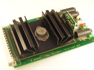
5. Final Product and Implementation
The culmination of the design and development process is the fully assembled inverter. This part showcases the final product in a real-world application, emphasizing the practical implementation of the developed PCB technology.
Conclusion
The development of inverter PCBs is a multifaceted process that requires a deep understanding of electronic principles, meticulous assembly techniques, and rigorous testing. The journey from basic design to the final product showcases the blend of innovation and precision engineering that drives modern inverter technology.