目录
ToggleAdvanced Techniques in High-Frequency PCB Design for 5G Applications
Introduction
As the world transitions to 5G technology, the demand for high-frequency PCB design has surged. The high-frequency nature of 5G signals requires PCBs that can handle increased data rates and higher signal integrity requirements. Advanced techniques in high-frequency PCB design are crucial to meet these demands. This article delves into key methods and strategies to optimize PCB performance for 5G applications.
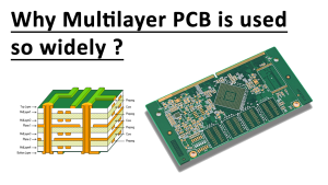
Controlled Impedance for Signal Integrity
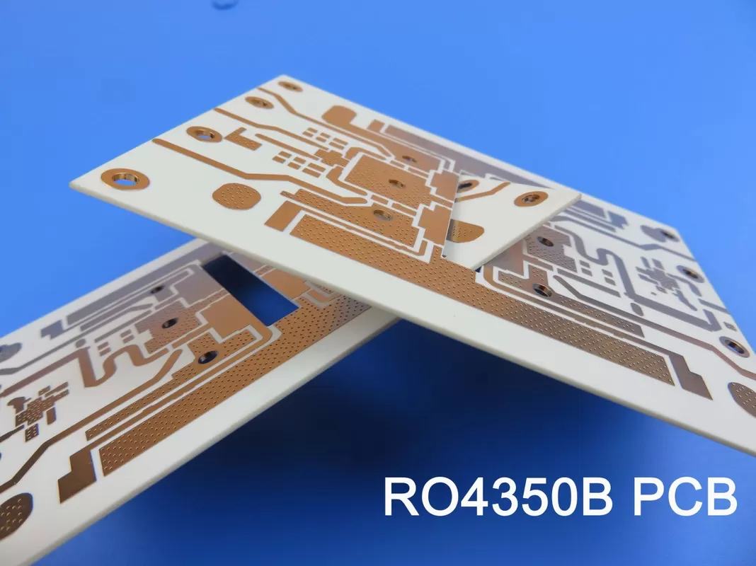
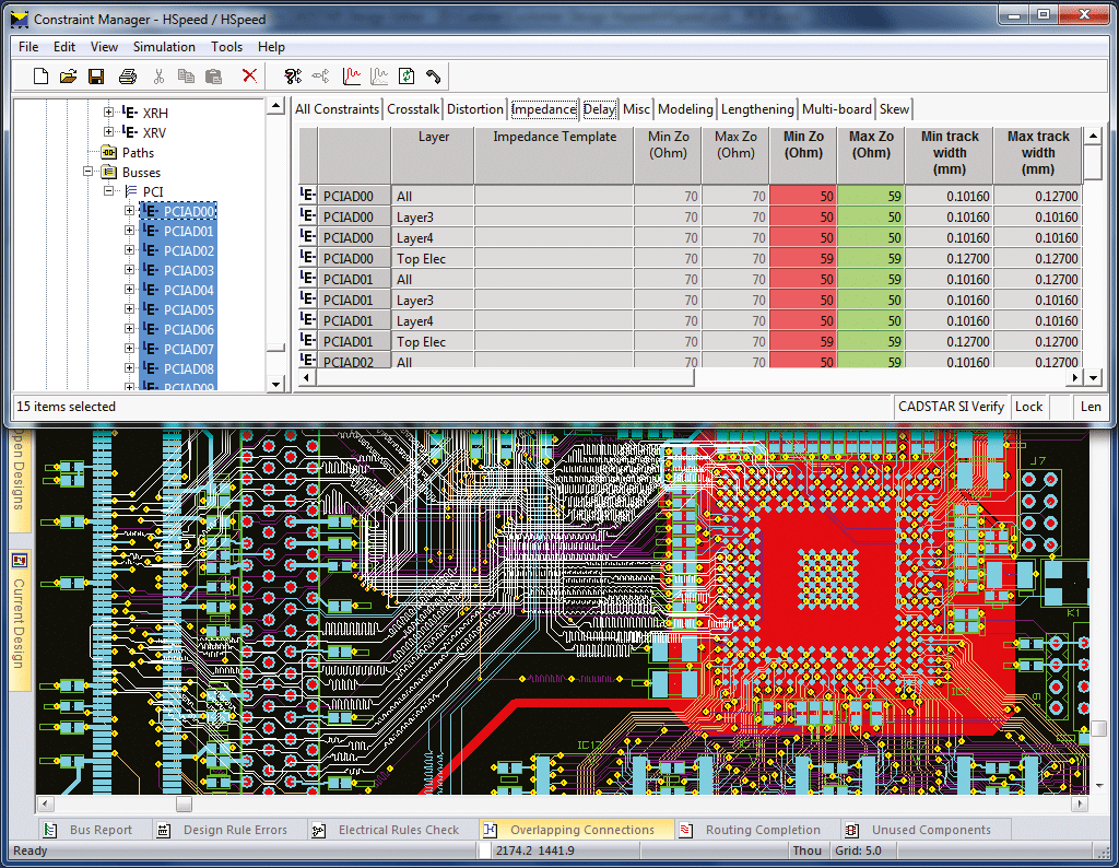
In high-frequency PCB design, controlled impedance is essential to maintain signal integrity. This technique ensures that the impedance of transmission lines matches the source and load, minimizing signal reflection and loss. Engineers achieve controlled impedance by carefully selecting the PCB substrate materials and precisely controlling the trace width and spacing. For 5G applications, materials with low dielectric constants and loss tangents, such as PTFE and Rogers laminates, are preferred.
Material |
Dielectric Constant (Dk) |
Loss Tangent (Df) |
Frequency Range |
|---|---|---|---|
|
PTFE |
2.1 |
0.0004 |
Up to 10 GHz |
|
Rogers |
3.48 |
0.004 |
Up to 10 GHz |
Differential Pair Routing
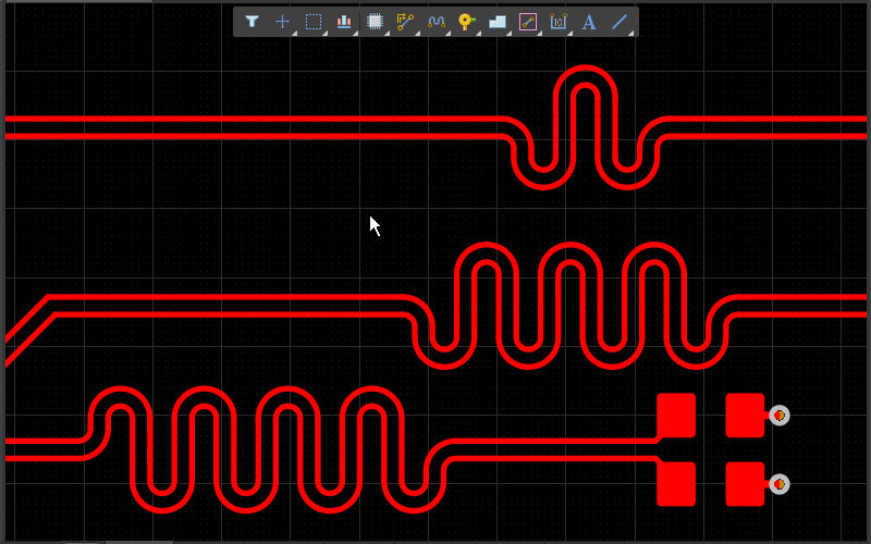
Differential pair routing is another crucial technique in high-frequency PCB design for 5G applications. This method involves routing pairs of signal traces that carry equal and opposite signals, effectively reducing electromagnetic interference (EMI) and crosstalk. The key to successful differential pair routing lies in maintaining consistent trace spacing and length matching to ensure signal integrity.
Routing Type |
EMI Susceptibility |
Signal Integrity |
Crosstalk |
|---|---|---|---|
|
Single-ended |
High |
Moderate |
High |
|
Differential Pair |
Low |
High |
Low |
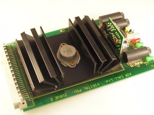
Thermal Management Techniques
Effective thermal management is critical in high-frequency PCB design, especially for 5G applications where high data rates generate significant heat. Techniques such as thermal via arrays, heat sinks, and advanced PCB materials with high thermal conductivity are employed to manage heat dissipation. Proper thermal management not only ensures reliable performance but also extends the lifespan of the PCB.
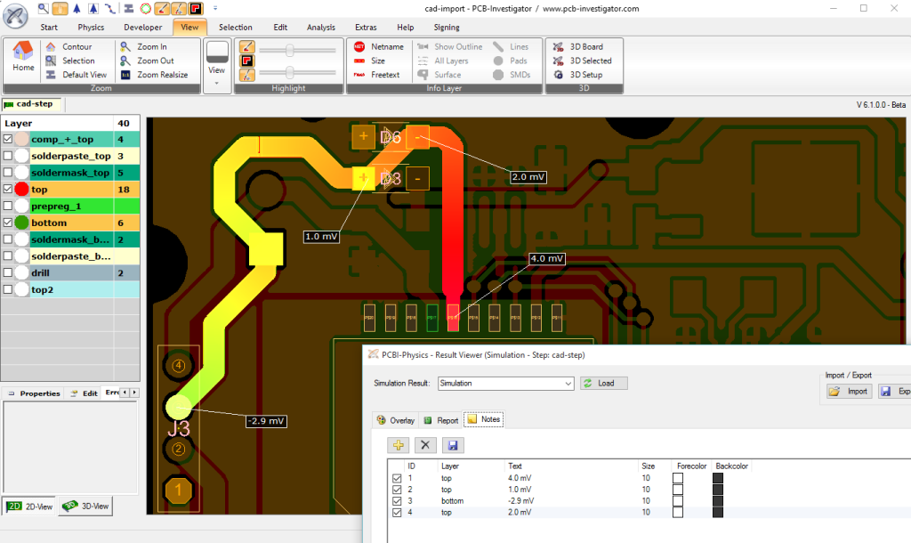
Use of Signal Integrity Simulation Tools
To ensure robust high-frequency PCB design, engineers utilize signal integrity simulation tools. These tools, such as ANSYS HFSS and Keysight ADS, allow designers to model and analyze the PCB’s electrical performance under various conditions. By simulating the PCB design, engineers can identify and mitigate potential issues such as signal distortion, impedance mismatches, and EMI before the actual fabrication.

Material Selection for High-Frequency PCBs
Choosing the right materials is fundamental to achieving high-frequency performance in PCBs. Materials like PTFE, Rogers, and other low-loss substrates are preferred due to their excellent electrical properties. These materials minimize signal loss and ensure stable performance at high frequencies, making them ideal for 5G applications.
Material |
Dielectric Constant (Dk) |
Loss Tangent (Df) |
Thermal Conductivity (W/mK) |
|---|---|---|---|
|
PTFE |
2.1 |
0.0004 |
0.25 |
|
Rogers |
3.48 |
0.004 |
0.5 |
Conclusion
Advanced techniques in high-frequency PCB design are essential for optimizing performance in 5G applications. By employing controlled impedance, differential pair routing, effective thermal management, and utilizing signal integrity simulation tools, engineers can ensure that their PCB designs meet the stringent requirements of 5G technology. The careful selection of high-performance materials further enhances the reliability and efficiency of these PCBs.