目录
ToggleAdvanced Signal Integrity Techniques for High-Speed PCB Design
Introduction
In the realm of high-speed PCB design, maintaining signal integrity is paramount. As data rates increase and circuits become more compact, the challenges associated with signal degradation, crosstalk, and electromagnetic interference (EMI) intensify. To ensure reliable signal transmission, engineers must adopt advanced signal integrity techniques that encompass meticulous design practices and sophisticated analytical tools. This article delves into key strategies and methods employed in high-speed PCB design to enhance signal integrity, from impedance control to simulation techniques.
The Importance of Controlled Impedance
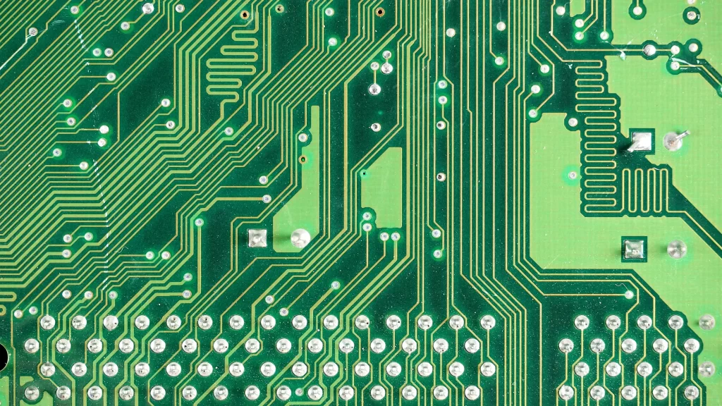
Controlled Impedance in High-Speed PCB Design
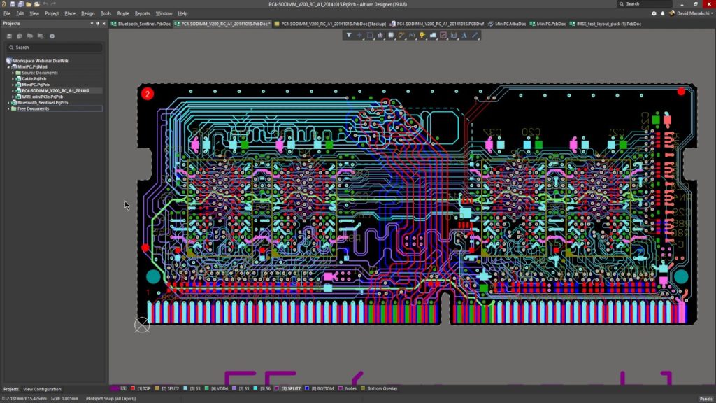
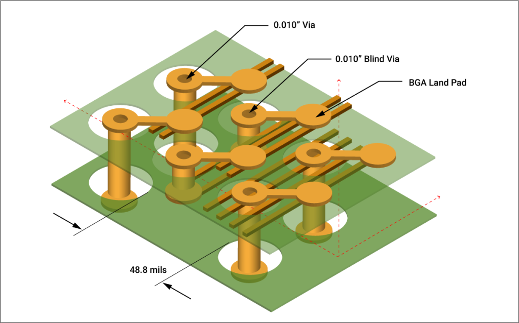
One of the fundamental aspects of ensuring signal integrity in high-speed PCB designs is controlled impedance. As signals propagate through PCB traces, their impedance must remain consistent to prevent reflections and signal loss. Variations in impedance can lead to significant signal integrity issues, including waveform distortion and increased jitter. Controlled impedance is achieved by meticulously designing the trace width, spacing, and the dielectric properties of the substrate. For instance, maintaining a differential impedance of 100 ohms for high-speed differential pairs is crucial for minimizing reflections and ensuring signal integrity.
To accurately achieve controlled impedance, engineers must consider the following:
- Trace Geometry: Adjusting trace width and spacing to achieve the desired impedance.
- Dielectric Properties: Selecting PCB materials with consistent dielectric constants.
- Stack-Up Design: Optimizing the layer stack-up to provide stable reference planes and controlled impedance.
Advanced Routing Techniques
Differential Pair Routing
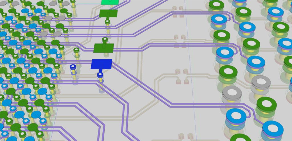
Differential pair routing is essential in high-speed PCB design to enhance signal integrity. This technique involves routing two complementary signals in close proximity to each other, which helps to cancel out noise and minimize electromagnetic interference. Key considerations for differential pair routing include:
- Equal Trace Lengths: Ensuring both traces in a pair have identical lengths to avoid skew.
- Consistent Spacing: Maintaining uniform spacing between the traces to preserve differential impedance.
- Minimized Crosstalk: Keeping differential pairs away from other signal traces to reduce crosstalk.
These practices help maintain signal integrity by ensuring that differential signals are accurately transmitted, reducing susceptibility to external noise and interference.
Signal Integrity Simulation Tools
Utilizing Signal Integrity Simulation
Signal integrity simulation tools are invaluable in high-speed PCB design, allowing engineers to model and analyze signal behavior before physical prototyping. Tools like HyperLynx, SIwave, and CST Studio Suite enable the simulation of various signal integrity aspects, including:
- Reflection Analysis: Identifying and mitigating signal reflections caused by impedance discontinuities.
- Crosstalk Prediction: Modeling crosstalk between adjacent traces to design effective mitigation strategies.
- Eye Diagram Analysis: Assessing signal quality through eye diagrams to evaluate timing and voltage margins.
These simulations provide insights into potential signal integrity issues, enabling engineers to make informed design decisions and optimize PCB layouts for high-speed applications.
Impedance Matching Techniques
Effective Impedance Matching
Impedance matching is crucial in high-speed PCB design to ensure seamless signal transmission between different components and traces. Mismatched impedance can cause reflections, leading to signal degradation. Techniques for impedance matching include:
- Stub Tuning: Adjusting trace stubs to cancel out reflections at specific frequencies.
- Terminations: Using series or parallel terminations to match impedance at trace ends.
- Baluns: Implementing baluns to match impedance between unbalanced and balanced transmission lines.
These methods help to maintain signal integrity by ensuring that impedance discontinuities are minimized, thereby reducing reflections and maintaining signal quality.
Managing Crosstalk
Crosstalk Mitigation Strategies
Crosstalk between adjacent signal traces can significantly affect signal integrity in high-speed PCB designs. Effective crosstalk mitigation strategies include:
- Shielding: Using ground planes and shielding traces to isolate critical signal paths.
- Spacing: Increasing the distance between parallel traces to reduce mutual coupling.
- Guard Traces: Placing guard traces between high-speed signal lines to absorb crosstalk.
Implementing these strategies helps to minimize crosstalk, ensuring that signal transmission remains clean and interference-free.
Conclusion
Maintaining signal integrity in high-speed PCB design is a multifaceted challenge that requires a combination of controlled impedance, advanced routing techniques, simulation tools, impedance matching, and crosstalk mitigation. By employing these advanced signal integrity techniques, engineers can design PCBs that meet the stringent performance requirements of modern high-speed applications. As technology continues to advance, the importance of robust signal integrity practices will only grow, making it essential for PCB designers to stay abreast of the latest developments in the field.
Data Table: Key Signal Integrity Techniques
| Technique | Description | Key Benefit |
|---|---|---|
| Controlled Impedance | Designing traces with consistent impedance | Minimizes reflections |
| Differential Pair Routing | Routing complementary signals together | Reduces noise and EMI |
| Signal Integrity Simulation | Modeling signal behavior before physical testing | Identifies potential issues early |
| Impedance Matching | Ensuring impedance consistency across components | Reduces signal reflections |
| Crosstalk Mitigation | Techniques to reduce interference between traces | Enhances signal clarity |