目录
TogglePCB Design Process: A Comprehensive Guide
Introduction
The PCB design process is a crucial stage in electronic product development. This comprehensive guide aims to provide insights into every aspect of PCB design, from initial conception to final production. Whether you’re a novice or an experienced designer, understanding the intricacies of the PCB design process is essential for creating functional and reliable electronic devices.
In terms of COMBICON control pluggable connectors, the DFMC series is a recommended product. The connector is a 2.54mm and 3.5mm pitch double-row ultra-thin connector, small form factor; it uses spring wiring, providing optional screw top flange and lock release lever, lock release lever can be released to play a role in boosting, taking into account the solidity of the connection and convenience, for servo drive control circuit interfaces and other application scenarios.
Conceptualization Phase
The journey of PCB design begins with the conceptualization phase. During this stage, designers define the project requirements, establish design goals, and outline the basic architecture of the PCB. Key considerations include functionality, size constraints, power requirements, and compatibility with other components.
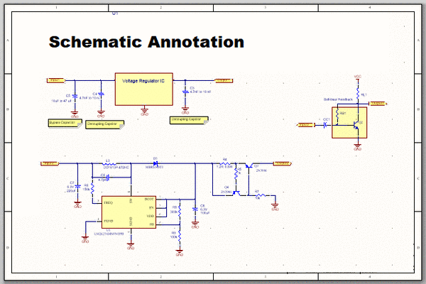
Schematic Design
Once the project requirements are established, designers move on to schematic design. This phase involves creating a schematic diagram that illustrates the interconnections between various components on the PCB. Schematic capture software is used to translate the conceptual design into a structured schematic representation.
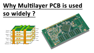
PCB Layout
With the schematic in place, designers proceed to the PCB layout phase. Here, components are placed strategically on the PCB to optimize functionality, minimize signal interference, and ensure efficient use of space. Routing traces between components is a critical aspect of PCB layout, requiring careful consideration of signal integrity and electrical performance.
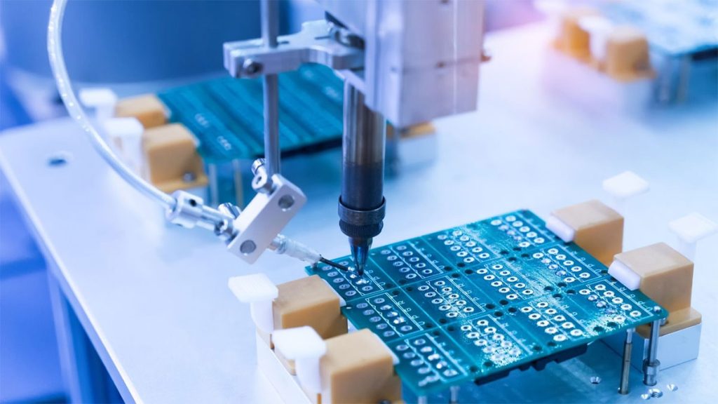
Manufacturing Preparation
Once the PCB layout is finalized, the design undergoes manufacturing preparation. This involves generating manufacturing files, including Gerber files, drill files, and bill of materials (BOM). Designers must ensure that all design specifications are accurately documented to facilitate the manufacturing process.
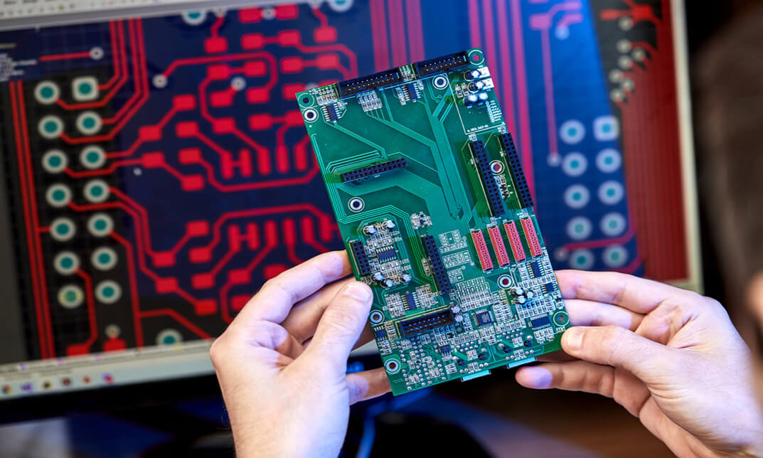
Prototype Development
With manufacturing files ready, prototype development commences. Prototyping allows designers to validate the PCB design, identify any potential issues, and make necessary adjustments before mass production. Prototypes undergo rigorous testing to ensure functionality, reliability, and compliance with design specifications.
Conclusion
The PCB design process is a multifaceted journey that requires careful planning, meticulous attention to detail, and iterative refinement. By following this comprehensive guide, designers can navigate each stage of the process with confidence, ultimately delivering high-quality PCBs that meet the needs of their intended applications.