目录
ToggleHigh-Speed PCB Design: Key Performance Considerations
In high-speed PCB design, optimizing performance and reliability is essential. This article explores key considerations such as impedance matching, signal integrity, EMI/EMC, and grounding techniques.
1. Impedance Matching in PCB Design:
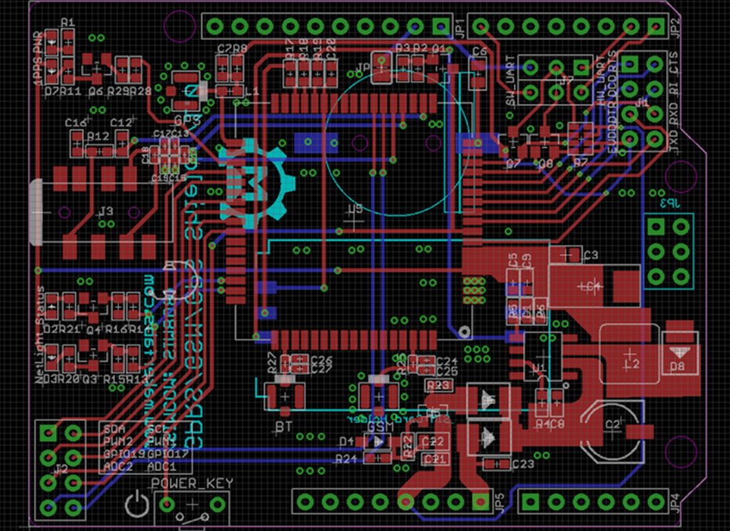
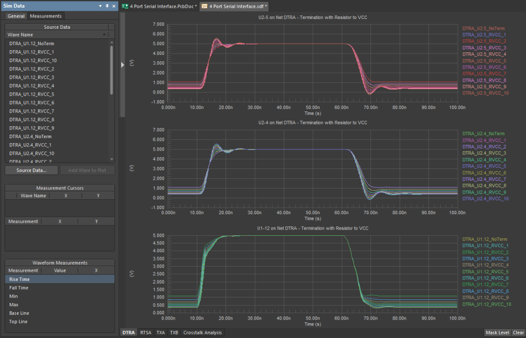
Impedance matching is a critical factor in high-speed PCB design. The impedance values are closely related to the routing methods, such as microstrip or stripline, distance from reference layers (power or ground planes), trace width, PCB material, etc. It’s essential to note that impedance values are determined after routing. Simulation software may not always account for impedance mismatches accurately due to limitations in line models or mathematical algorithms. In the schematic design phase, incorporating terminators like series resistors can help mitigate impedance mismatch effects. However, the fundamental solution lies in careful routing to avoid impedance mismatches.
2. Segregating Digital and Analog Grounds:
It’s common practice to separate digital and analog grounds in PCBs containing multiple digital/analog functional blocks. This segregation is crucial because digital circuits generate noise in power and ground planes during high-low voltage transitions. If digital and analog ground planes are not segregated, the significant noise produced by digital circuitry can interfere with analog signals, even if they are physically distant. Therefore, segregating digital and analog grounds is essential, particularly when analog circuits are in close proximity to areas generating significant digital noise.
3. Considering EMC/EMI Rules in High-Speed PCB Design:
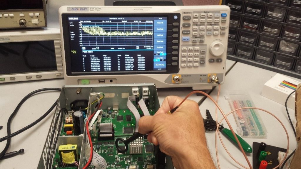
Effective EMI/EMC design requires addressing both radiated and conducted emissions. While radiated emissions concern higher frequencies (>30MHz), conducted emissions involve lower frequencies (<30MHz). Neglecting either frequency range can compromise EMC compliance. A comprehensive EMC/EMI design strategy involves planning component placement, PCB layer stack-up, routing paths, component selection, etc., during the layout phase. Adhering to these considerations preemptively minimizes the need for costly post-design modifications.
4. Grounding Techniques to Reduce Interference:
To minimize interference, ground traces should not form closed loops but rather adopt a branching configuration. Additionally, maximizing ground plane area aids in reducing interference.
5. Adjusting Routing Topology to Enhance Signal Integrity:
Optimizing routing topology to enhance signal integrity is complex and depends on factors like signal directionality, signal types (uni/bi-directional), voltage levels, etc. Selecting the appropriate topology for signal integrity requires a deep understanding of circuit principles, signal types, and routing challenges.
6. Ensuring Stability for Signals Above 100M:
For signals exceeding 100M, stability relies on minimizing the impact of transmission lines on signal quality. This entails keeping signal traces short and employing different strategies for maintaining signal quality based on signal types such as TTL, GTL, LVTTL