目录
ToggleUnderstanding the Basics: Key Considerations in PCB Design
PCB design is a critical aspect of electronic product development, and it plays a crucial role in determining the overall performance and reliability of the final product. To achieve success in PCB design, it is essential to understand the basics and key considerations involved in the process.
One of the fundamental aspects of PCB design is component placement. Proper component placement is crucial for ensuring signal integrity, minimizing noise, and optimizing thermal management. It is important to consider the proximity of components to each other, as well as their relationship to critical signal paths and heat-generating components. By carefully planning the component placement, designers can minimize signal interference and thermal issues, leading to improved overall performance.
Another key consideration in PCB design is trace routing. The routing of traces on a PCB determines the flow of signals and power throughout the circuit. It is important to ensure that traces are properly routed to avoid signal degradation, crosstalk, and electromagnetic interference. Designers should pay attention to trace widths, spacing, and impedance matching to optimize signal integrity and minimize signal loss.
Power distribution is yet another critical consideration in PCB design. Proper power distribution ensures that all components receive the required power without voltage drops or noise. Designers should carefully plan the power distribution network, including the placement of power planes, decoupling capacitors, and power traces. By optimizing the power distribution, designers can prevent power-related issues such as voltage fluctuations and noise, which can negatively impact the performance and reliability of the PCB.
Overcoming Design Challenges: Common Pitfalls to Avoid
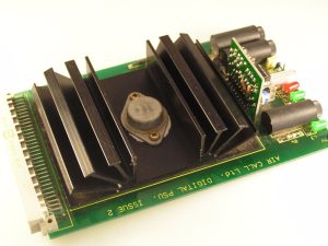
While designing a PCB, there are several common pitfalls that designers should be aware of and avoid. One common pitfall is inadequate thermal management. Heat dissipation is a significant concern in electronic circuits, and failure to address it can lead to component failure and reduced lifespan. Designers should consider the thermal characteristics of components and plan for proper heat sinking, thermal vias, and thermal relief pads to ensure efficient heat dissipation.
Another common pitfall is overlooking design for manufacturability (DFM) guidelines. DFM guidelines provide recommendations for designing PCBs that are easy to manufacture and assemble. Ignoring these guidelines can result in increased manufacturing costs, delays, and potential quality issues. Designers should familiarize themselves with DFM guidelines and incorporate them into their design process to ensure a smooth transition from design to production.
Signal integrity issues are also common pitfalls in PCB design. High-speed signals are susceptible to noise, reflections, and impedance mismatches, which can lead to signal degradation and data errors. Designers should carefully consider signal integrity principles, such as controlled impedance routing, proper termination techniques, and signal integrity simulations, to ensure reliable signal transmission.
Optimization Techniques: Tips for Achieving PCB Design Success
To achieve success in PCB design, designers can employ various optimization techniques. One such technique is the use of advanced design software and tools. Modern PCB design software offers features such as auto-routing, design rule checks, and simulation capabilities, which can significantly streamline the design process and help identify potential issues early on. By leveraging these tools, designers can save time, reduce errors, and optimize their designs for better performance.
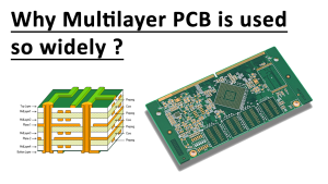
Another optimization technique is the use of multi-layer PCBs. Multi-layer PCBs provide additional routing space and allow for better signal integrity and thermal management. By utilizing multiple layers, designers can reduce the complexity of routing, minimize signal interference, and improve overall performance.
Designers can also optimize their PCB designs by considering the use of surface mount technology (SMT). SMT components are smaller, lighter, and offer better electrical performance compared to through-hole components. By utilizing SMT components, designers can achieve higher component density, reduce signal path lengths, and improve overall reliability.
Best Practices for Efficient and Error-Free PCB Design
To ensure efficient and error-free PCB design, designers should follow best practices throughout the design process. One best practice is to start with a clear design specification. A well-defined design specification helps in setting clear goals, identifying design constraints, and ensuring that the final design meets the desired requirements.
Another best practice is to perform thorough design reviews. Design reviews involve a critical evaluation of the design by a team of experts to identify potential issues and suggest improvements. By conducting regular design reviews, designers can catch errors early on, improve the design quality, and reduce the risk of costly rework.
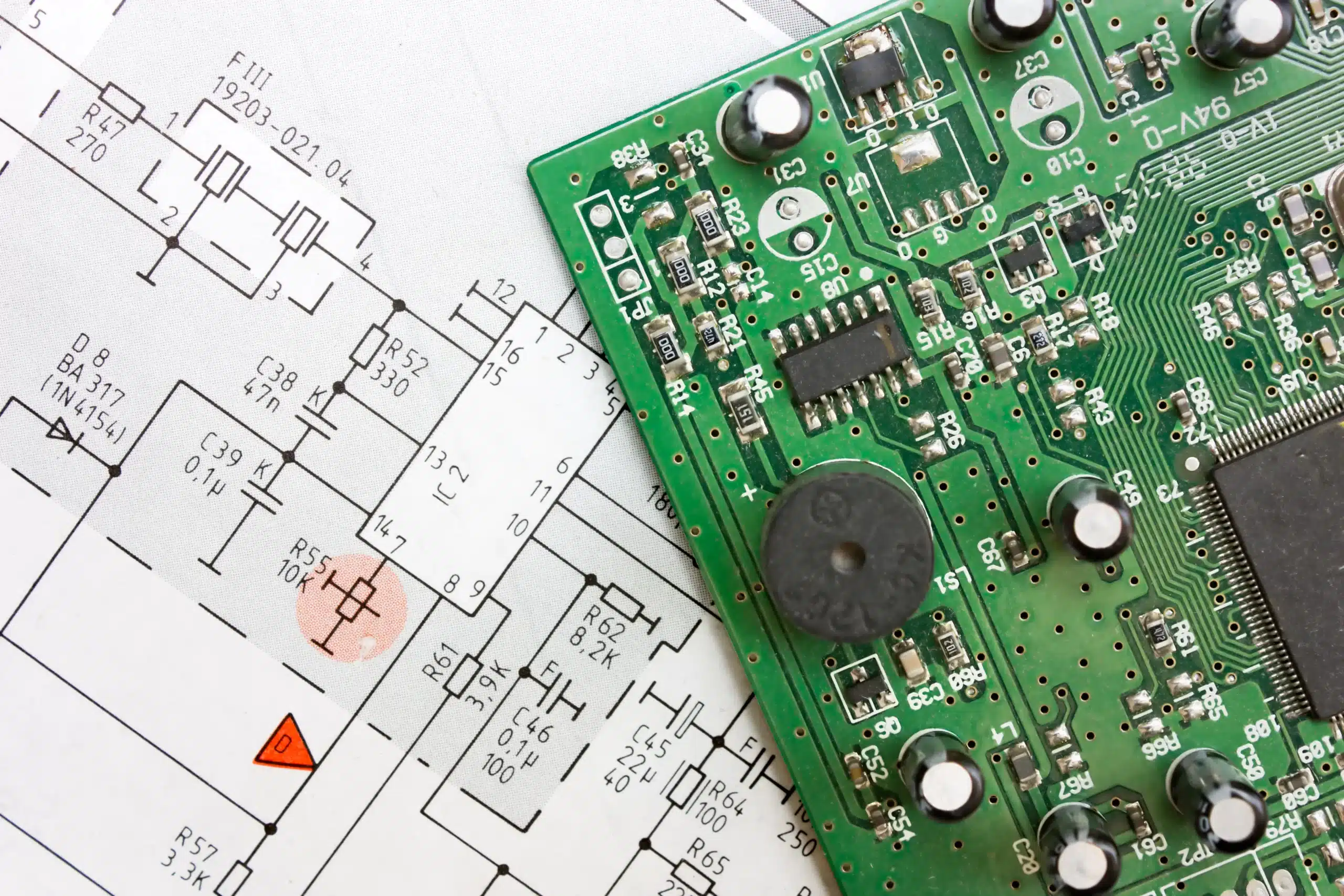
Documentation is also a crucial aspect of efficient PCB design. Maintaining accurate and up-to-date documentation, including schematics, layout files, and bill of materials (BOM), helps in ensuring proper communication with manufacturers and facilitates future design modifications or repairs.
In conclusion, avoiding common pitfalls in PCB design is essential for achieving optimization and success. By understanding the basics, overcoming design challenges, employing optimization techniques, and following best practices, designers can create efficient and error-free PCB designs that meet the desired performance, reliability, and manufacturability requirements.
PCB Fabrication
https://www.facebook.com/profile.php?id=100086889766737