目录
ToggleA Deep Dive into 4-Layer PCBs: Design, Materials, and Applications
Introduction to 4-Layer PCBs
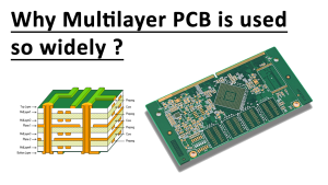
4-Layer PCBs represent a step-up in complexity from 2-layer boards, offering improved performance for more demanding applications. These boards consist of four conductive copper layers, providing greater flexibility in design and enhanced signal integrity.
Design Process of 4-Layer PCBs
The design of a 4-layer PCB requires careful planning to optimize layer stack-up, signal routing, and power distribution. Advanced CAD software is utilized to create precise and efficient designs, considering factors like impedance control and EMI shielding.
Materials Used in 4-Layer PCBs
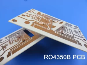
The choice of materials is crucial in determining the board’s performance. Typical materials include FR4 for the substrate, copper for the conductive layers, and various dielectrics to ensure proper insulation between layers.
Manufacturing Process
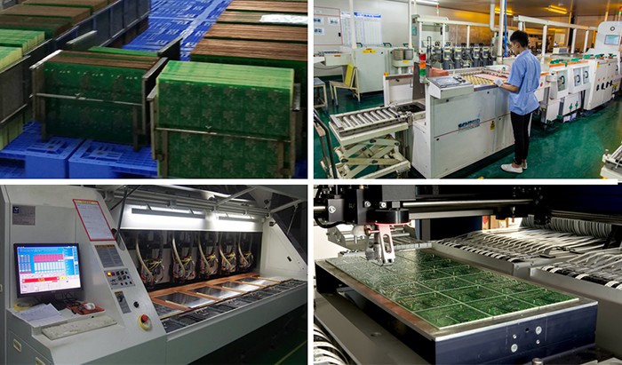
The production of 4-layer PCBs involves complex processes such as lamination, drilling, plating, and etching to create precise multilayer structures. Attention to detail is key to ensuring the quality and reliability of the final product.
Basic Parameters of 4-Layer PCBs
| Parameter | Description |
|---|---|
| Layer Count | 4 |
| Material | Typically FR4 |
| Board Thickness | Commonly 1.6 mm |
| Copper Thickness | 1 oz per square foot as standard |
| Minimum Trace Width | Typically 0.1 mm (4 mil) |
| Minimum Hole Size | Usually 0.3 mm (12 mil) |
| Surface Finish | Options like HASL, ENIG, OSP |
| Solder Mask | Available in various colors |
This table provides a general overview of the specifications for a standard 4-Layer PCB.
Applications of 4-Layer PCBs
4-layer PCBs find applications in more complex electronic devices, including consumer electronics, automotive systems, and industrial machinery. Their ability to handle higher densities and more intricate circuit designs makes them ideal for these applications.
Conclusion
4-Layer PCBs are essential in the electronics industry, catering to a wide range of applications that require higher circuit complexity and performance. They strike a balance between cost, performance, and size, making them a popular choice for medium-complexity electronic devices.
-
Optimizing Signal Integrity in Multi-layer PCBs for High-Speed Data Transfer
-
Optimizing Thermal Management in High-Density PCB Layouts
-
Advanced Techniques in High-Frequency PCB Design for 5G Applications
-
Eco-Friendly Approaches in PCB Manufacturing: Reducing Environmental Impact
-
Emerging Trends in PCB Manufacturing: From Traditional Methods to Cutting-Edge Innovations


